Building a circuit board (PCB) is a fundamental skill for anyone interested in electronics and DIY projects. Whether you\’re a hobbyist, a student, or a professional, understanding how to create a functional PCB can open doors to numerous opportunities. In this article, we\’ll walk you through the process of building a circuit board from scratch, including the necessary materials, steps, and best practices.
Materials and Tools Required
Before you get started, you will need to gather the essential materials and tools. Here\’s a list of what you\’ll need:
- PCB Board: The base material, typically made of fiberglass or composite epoxy.
- Design Software: Tools like Eagle, KiCad, or Altium for designing the circuit layout.
- Copper Clad Board: A board coated with a thin layer of copper where the circuit will be etched.
- Etching Solution: Ferric chloride or an alternative for removing unwanted copper.
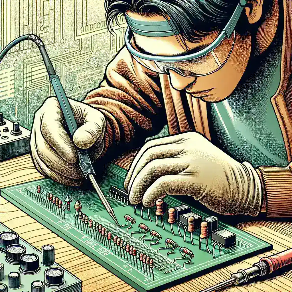
- Soldering Iron: A tool to solder components onto the board.
- Solder: Metal alloy used to join electronic components to the PCB.
- Drill: For making holes to place components.
- Components: Resistors, capacitors, ICs, and other necessary electronic parts.
- Protective Gear: Gloves and safety glasses for safety.
Steps to Build a Circuit Board
Step 1: Designing the Circuit
Start by designing your circuit using PCB design software. Here is where you plan out the electrical connections, component placement, and trace routes. Most software will allow you to create a schematic diagram and then convert it into a PCB layout.
Step 2: Printing the Design
Once the design is ready, print it out onto a transparent sheet. This printout will be used to transfer the design onto the copper-clad board.
Step 3: Transferring the Design
Place the transparent sheet with the printed circuit design onto the copper-clad board. Use an iron to transfer the design by applying heat. Ensure even pressure and heat to make sure the design transfers correctly.
Step 4: Etching the Board
Submerge the copper-clad board into the etching solution. The solution will remove the exposed copper, leaving behind the desired circuit pattern. Make sure to follow safety guidelines when handling the etching solution.
Step 5: Drilling Holes
Once the etching process is complete, use a drill to make holes for the electronic components. Ensure that the holes are accurately positioned based on your design.
Step 6: Soldering Components
Now, place the electronic components into the drilled holes and solder them in place. Make sure to use proper soldering techniques to avoid cold joints or short circuits.
Step 7: Testing and Troubleshooting
Finally, test your circuit board by connecting it to a power source and other necessary appliances. Check for any errors or misplaced components and troubleshoot if needed.
Best Practices and Tips
Double-Check Designs
Before going ahead with etching, always double-check the design for any errors or omissions. Use software features like design rule checking (DRC) to catch potential issues.
Safety Precautions
Always follow safety guidelines, especially when handling chemicals like etching solutions. Use protective gear such as gloves and safety glasses.
Maintain Clean Work Area
A clean work area helps avoid contamination and errors. Keep your tools and materials organized and free from clutter.
Common Mistakes to Avoid
- Not double-checking designs before printing.
- Improper etching leading to incomplete circuit paths.
- Cold solder joints causing poor electrical connections.
- Incorrect component placement leading to malfunctioning circuits.
Conclusion
Building a circuit board may seem daunting, but with the right tools, materials, and steps, it becomes an approachable task. Whether for a professional project or a personal hobby, creating your own PCB is a rewarding experience that offers endless possibilities for innovation and problem-solving.